


MIT-Bengaluru taps CMTI to prepare semiconductor talent pipeline
Manipal Institute of Technology Bengaluru (MIT-Bengaluru), a constituent institution of Manipal Academy of Higher Education (MAHE), has decided to build a future-focused semiconductor talent pipeline through rare hands-on exposure to advanced chip fabrication environments and global semiconductor ecosystems.
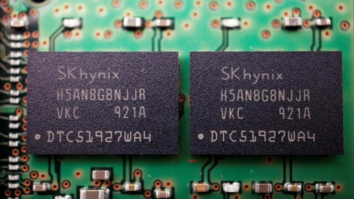
A group of select students from MIT Bengaluru recently underwent nearly 120 hours of specialised training inside a Class 100–10,000 clean-room facility at the Central Manufacturing Technology Institute (CMTI), in Bengaluru. The programme offered under-graduate students direct exposure to semiconductor fabrication processes that are typically inaccessible at the undergraduate level in India, according to MIT-Bengaluru.
The students received practical training across critical semiconductor manufacturing workflows, including wafer cleaning, etching, deposition, lithography, characterisation, integration and dicing. As part of the immersive learning experience, they also successfully manufactured a 600-micron MOS (Metal-Oxide-Semiconductor) capacitor, providing them with first-hand exposure to the complexities of chip fabrication and device engineering.
The initiative forms part of MIT Bengaluru’s broader push toward industry-integrated and experiential engineering education in emerging technology domains such as semiconductor fabrication, VLSI engineering, AI hardware systems, EV chip ecosystems, advanced electronics manufacturing and deep-tech product engineering.
Professor Madhu Veeraraghavan, Pro Vice-Chancellor, MAHE Bengaluru, said, “India’s semiconductor journey cannot be built on policy alone. It must be built on people, deep-tech innovations, advanced manufacturing capability and globally relevant talent ecosystems.
“Institutions must move beyond conventional learning models and create opportunities that prepare students for emerging technology sectors of national importance.
“Initiatives like this would reflect the kind of institution, industry and international collaboration that would determine whether India’s semiconductor ambitions translate into real engineering capability.”
Iven Jose, Director, MIT Bengaluru, emphasised the institution’s approach toward next-generation engineering education. “Unlike conventional engineering programmes that rely mainly on simulation-based learning, MIT Bengaluru emphasises impact-based teaching, project-driven learning, and industry-integrated pedagogy.
“This initiative reflects MIT-Bengaluru’s commitment to next-generation engineering education by enabling students to experience semiconductor fabrication environments, chip-processing workflows and real-world semiconductor ecosystems firsthand.”
Published – May 16, 2026 11:31 am IST